
Advanced 5G and key semiconductor materials
The wafer process uses advanced plasma etching, plasma coating and other related technologies and equipment, which has become the key to yield and productivity
The wafer process uses advanced plasma etching, plasma coating and other related technologies and equipment, which has become the key to yield and productivity.
Internet technology has become an indispensable part of modern life. Food, clothing, housing, transportation, education, and entertainment can all be achieved through Internet technology, so its related materials and processes will be closely related to our lives. , In view of the times, the center has invested a lot of research, introducing plasma etching and coating technology into key materials, reducing material volume, improving process accuracy, increasing conductivity and heat dissipation power, etc., so that the semiconductor industry can break through in a short time. Moore’s Law.
Flexible high frequency film type electromagnetic wave shielding film
For the new generation of 5G communication technology, in order to maintain the signal transmission quality of electronic product signals under high-speed transmission, as well as the demand for wider and higher frequency ranges, it will be an important challenge to avoid electromagnetic waves from interfering with signal transmission. In addition, as electronic components move towards miniaturization and flexibility, the demand for electromagnetic wave shielding materials to change from the traditional cavity-based metal cover to the soft -coated electromagnetic wave shielding film is increasing. Therefore, our center proposes to use high-power pulsed magnetron sputtering to grow high-quality copper metal thin films on polyurethane composite foils at low temperature . Through various analysis, it can be seen that the average electromagnetic wave shielding efficiency in the X band is -60 dB, coupled with excellent flexural durability , so it has the absolute advantage of replacing the existing commercial soft high-frequency laminated electromagnetic wave shielding film products.
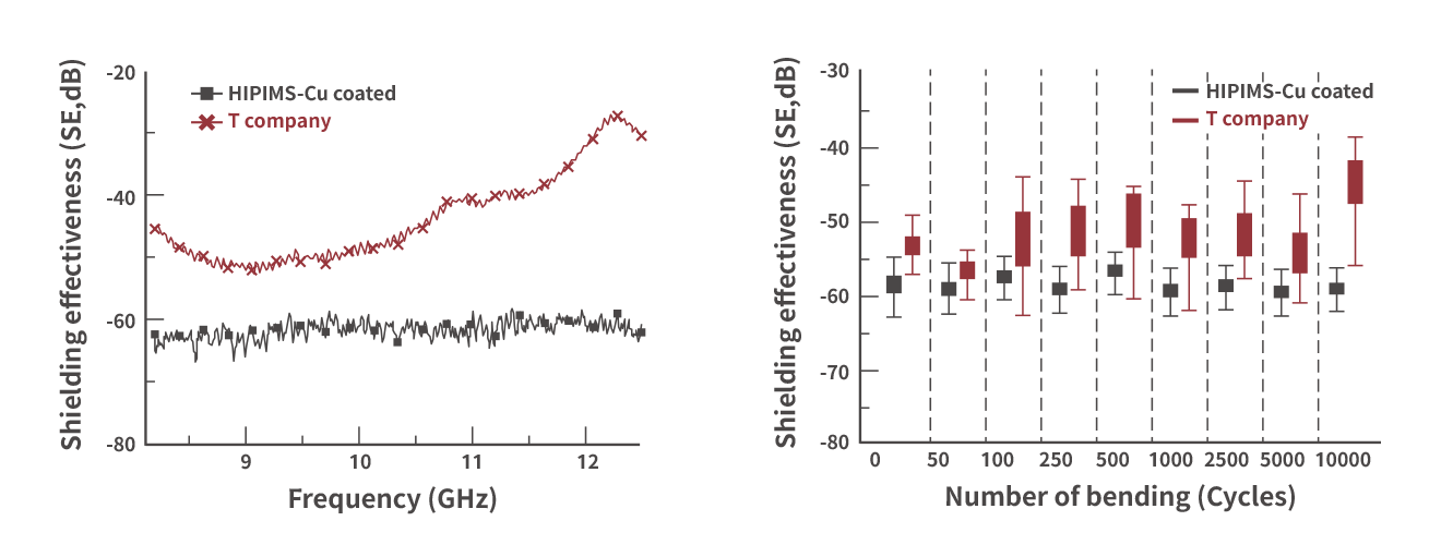
The electromagnetic wave shielding efficiency performance of HIPIMS-Cu flexible high-frequency electromagnetic wave shielding film and commercially available products in X band / Efficiency performance after dynamic deflection test at a curvature radius of 2.5 mm
Low dielectric loss high frequency flexible copper foil substrate
As electronic products gradually tend to be light, thin, short, mobile and highly functional, the overall electronic industry technology is advancing towards the goals of high frequency, high speed and thinning ; among them, the flexible copper foil substrate is one of the main materials of flexible printed circuit boards. It is mainly composed of polymer base material, adhesive and copper metal layer. At present, there are three main sources of copper metal layer: electrolytic copper foil, rolled copper foil , and electroplating/sputtering copper film. However, considering the process cost and the rising awareness of environmental protection, it is necessary to seek low-temperature, low-cost and green process alternatives as an urgent technology. Therefore, our center has developed the use of roll – to – roll airflow sputtering to directly grow copper metal films on liquid crystal polymer flexible boards. Based on airflow sputtering, it has the advantages of low-temperature and high-speed growth of thin films (the growth rate of thin films is more than 10 times that of traditional magnetron sputtering ). ); in addition, it does not need to use adhesive to bond the copper metal layer to the flexible board, so it can reduce the transmission loss of high-frequency signals on the flexible board circuit, so as to reduce the delay and distortion of the signal. Therefore, this technology is highly competitive in high-frequency flexible copper foil substrates .

Roll-to-roll airflow sputtering directly grows the adhesion of copper metal film on soft board
High Conductivity Thermal Graphene Copper Foil
Graphene is an emerging material that combines many excellent properties. However, from the perspective of obtaining continuous large-area graphene films , chemical vapor deposition is the only mass production method currently used in the industry, but its process temperature is often above 1000oC, and It is necessary to use an explosive chemical atmosphere. Therefore, in recent years, there have been studies on the feasibility of growing graphene films by physical vapor deposition . The center has successfully used high-power pulsed magnetron sputtering with plasma characteristics such as high ionization rate and high ion energy to grow graphene films on copper foils at 600oC ; it was further found that the graphene films were made of In The unique structure of -plane layered graphene and out-of-plane turbostratic graphene co -constructs, so its thermal diffusivity increases from 0.7 cm2/s of copper foil to 1.1 cm2/s. If copper atoms are doped in the graphene film process, the thermal diffusivity can be further increased to >2.0 cm2/s. Therefore, the graphene copper foil will effectively solve the hotspot problems derived from high frequency, high speed and high power semiconductor devices, thereby improving the service life and performance of the semiconductor devices.
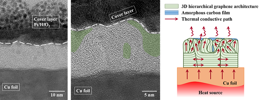
High-power pulsed magnetron sputtering of graphene films on copper foil with high-resolution penetrating electron microscope image and heat dissipation path
Application of Silicon Carbide Thin Films to Resist Plasma Etching in Semiconductors
This technology is jointly developed by the center and Dayong Vacuum Equipment Co., Ltd.
The localization of semiconductor-related industries is one of the goals that my country is currently promoting. During the plasma etching process of the semiconductor process, how to prevent the plasma atmosphere from affecting the vacuum pipeline, focus ring, vacuum chamber and spare parts in the machine Erosion generates dust, which causes cavity pollution, shortens the service life of components, and even contaminates silicon wafers, which in turn affects etching efficiency, wafer characteristics and yield, etc., which is a very important issue. To this end, our center proposes to use airflow sputtering technology to grow silicon carbide thin films on silicon focus rings at high speed, and it is proved that it can effectively reduce the etching speed by more than 10 times in SiF6+Cl2 plasma etching atmosphere. In addition, the growth rate of silicon carbide film grown by airflow sputtering can be greater than 10 μm /h (experimental machine), and the thickness of the obtained silicon carbide film can exceed 150 μm , so it has the potential to replace high temperature chemical vapor deposition silicon carbide in semiconductor anti-electricity. High potential for slurry etching applications.
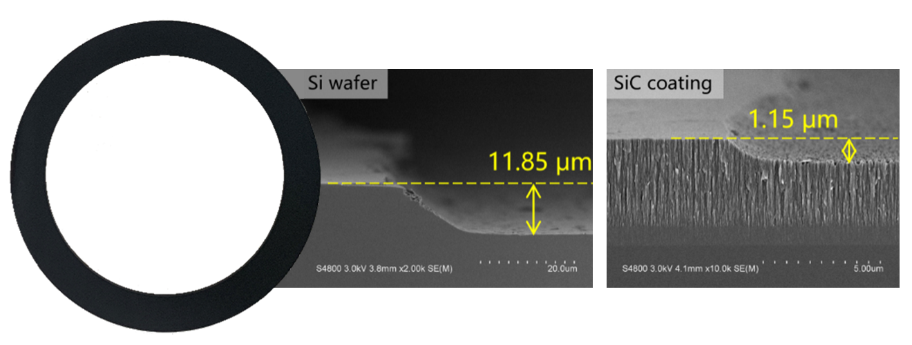
SiF6+Cl2 plasma etched silicon wafers and silicon carbide films